Look up nm or NM in Wiktionary, the free dictionary. NM, nm, and variations may refer to: Northwestern Mutual, financial services company in Wisconsin...
2 KB (343 words) - 04:24, 10 October 2023
In semiconductor manufacturing, the "3 nm" process is the next die shrink after the "5 nm" MOSFET (metal–oxide–semiconductor field-effect transistor) technology...
43 KB (3,620 words) - 01:23, 3 August 2024
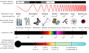
spelling as used by the International Bureau of Weights and Measures; SI symbol: nm), or nanometer (American spelling), is a unit of length in the International...
5 KB (409 words) - 15:47, 30 May 2024
defines the "5 nm" process as the MOSFET technology node following the "7 nm" node. In 2020, Samsung and TSMC entered volume production of "5 nm" chips, manufactured...
34 KB (2,855 words) - 04:47, 13 August 2024
25 nm on a nominally 65 nm process, while the pitch between two lines may be greater than 130 nm. For comparison, cellular ribosomes are about 20 nm end-to-end...
8 KB (794 words) - 03:16, 12 August 2024
manufacturing, the "2 nm process" is the next MOSFET (metal–oxide–semiconductor field-effect transistor) die shrink after the "3 nm" process node. The term...
29 KB (2,380 words) - 10:12, 14 August 2024
In semiconductor manufacturing, the "7 nm" process is a term for the MOSFET technology node following the "10 nm" node, defined by the International Roadmap...
51 KB (4,743 words) - 10:40, 6 August 2024
the MOSFET technology node that is the successor to the "22 nm" (or "20 nm") node. The "14 nm" was so named by the International Technology Roadmap for...
32 KB (2,759 words) - 09:11, 1 August 2024
The 250 nm process (250 nanometer process or 0.25 μm process) is a level of semiconductor process technology that was reached by most manufacturers in...
1 KB (102 words) - 02:29, 11 February 2024
The "22 nm" node is the process step following 32 nm in CMOS MOSFET semiconductor device fabrication. The typical half-pitch (i.e., half the distance between...
8 KB (801 words) - 00:51, 28 February 2024
nm (name mangling) is a Unix command used to dump the symbol table and their attributes from a binary executable file (including libraries, compiled object...
5 KB (444 words) - 17:42, 7 July 2023
The 800 nm process (800 nanometer process) is a level of semiconductor process technology that was reached in the 1987–1990 timeframe, by companies, such...
2 KB (173 words) - 18:13, 1 June 2024
10nm and 10 nm may refer to: 10 nm process, a die size first mainly produced in 2016 10 nm, an order of magnitude (length) This disambiguation page lists...
210 bytes (57 words) - 22:47, 6 February 2024
advancement over the previous 130 nm process. Eventually, it was succeeded by smaller process nodes, such as the 65 nm, 45 nm, and 32 nm processes. It was commercialized...
10 KB (875 words) - 03:00, 31 July 2024
The 180 nm process is a MOSFET (CMOS) semiconductor process technology that was commercialized around the 1998–2000 timeframe by leading semiconductor...
4 KB (350 words) - 01:50, 1 December 2023
The 130 nanometer (130 nm) process is a level of semiconductor process technology that was reached in the 2000–2001 timeframe by such leading semiconductor...
3 KB (267 words) - 15:14, 11 January 2024
Per the International Technology Roadmap for Semiconductors, the 45 nm process is a MOSFET technology node referring to the average half-pitch of a memory...
14 KB (1,395 words) - 00:52, 28 February 2024
The "28 nm" lithography process is a half-node semiconductor manufacturing process based on a die shrink of the "32 nm" lithography process. It appeared...
5 KB (447 words) - 01:57, 29 April 2024
The "32 nm" node is the step following the "45 nm" process in CMOS (MOSFET) semiconductor device fabrication. "32-nanometre" refers to the average half-pitch...
12 KB (1,213 words) - 22:04, 25 April 2024
The 350 nanometer process (350 nm process) is a level of semiconductor process technology that was reached in the 1995–1996 timeframe by leading semiconductor...
3 KB (208 words) - 05:23, 7 February 2024
The 600 nanometer process (600 nm process) is a level of semiconductor process technology that was reached in the 1994–1995 timeframe, by most leading...
1 KB (86 words) - 18:24, 21 October 2023


Albuquerque, New Mexico (redirect from Albuquerque, NM)
eastern portion of NM-528. Tramway Boulevard: Serves as a bypass around the northeastern quadrant, the route is designated as NM-556. Tramway Boulevard...
175 KB (15,490 words) - 12:59, 16 August 2024
"7 nm" processes are dimensionally similar to Intel's "10 nm" process. TSMC and Samsung's "10 nm" processes are somewhere between Intel's "14 nm" and...
21 KB (1,938 words) - 22:33, 6 June 2024
Processor and Core Solo Processor on 65 nm Process Datasheet Intel Core Duo Processor and Core Solo Processor on 65 nm Process Specification Update Intel Core...
469 KB (13,716 words) - 04:44, 18 August 2024

The NM-method or Naszodi–Mendonca method is the operation that can be applied in statistics, econometrics, economics, sociology, and demography to construct...
37 KB (5,368 words) - 17:33, 8 February 2024

NM-2201 (also known as CBL-2201 and NA-5F-PIC) is an indole-based synthetic cannabinoid that presumably has similar properties to the closely related 5F-PB-22...
7 KB (568 words) - 05:49, 2 June 2024
Euro.nm is a pan-European network of regulated markets dedicated to growth companies. Formed on March 1, 1996 by the European Association of European Emerging...
1 KB (128 words) - 07:43, 12 March 2021

Santa Fe, New Mexico (redirect from Santa Fe, NM)
"Santa Fe Southern Railway, Santa Fe, NM". Sfsr.com. Archived from the original on May 6, 2015. "Santa Fe, NM". Ghostdepot.com. Archived from the original...
93 KB (8,932 words) - 08:46, 15 August 2024
NM Nazmul Ahsan was a Bengali student who died fighting in the Bangladesh Liberation War. He is considered a martyr (Shaheed) in Bangladesh. He was awarded...
3 KB (219 words) - 07:15, 3 June 2024