Embedded DRAM (eDRAM) is dynamic random-access memory (DRAM) integrated on the same die or multi-chip module (MCM) of an application-specific integrated...
5 KB (418 words) - 04:49, 30 June 2023
456 MHz 512 MB of eDRAM Video Memory (16 × 32 MB) (The "I-32" Graphics Synthesizer was a custom variant that contained 32 MB of eDRAM instead of the typical...
3 KB (342 words) - 02:43, 1 July 2024
once. Graphics processing is handled by the ATI Xenos, which has 10 MB of eDRAM. Its main memory pool is 512 MB in size. Xbox 360 took a different approach...
46 KB (4,965 words) - 23:24, 1 July 2024

embedded DRAM (eDRAM). At the same time, 1T-SRAM has performance comparable to SRAM at multi-megabit densities, uses less power than eDRAM and is manufactured...
7 KB (840 words) - 15:56, 2 January 2024

East Fishkill, New York, using 45 nm SOI-technology and embedded DRAM (eDRAM) for caches. While unverified by Nintendo, hackers, teardowns, and unofficial...
11 KB (752 words) - 07:00, 21 July 2024
even any level, sometimes some latter or all levels are implemented with eDRAM. Other types of caches exist (that are not counted towards the "cache size"...
96 KB (13,277 words) - 09:33, 9 June 2024

Kryder's law Volatile RAM Hardware cache CPU cache Scratchpad memory DRAM eDRAM SDRAM SGRAM LPDDR QDRSRAM EDO DRAM XDR DRAM RDRAM DDR GDDR HBM SRAM 1T-SRAM...
80 KB (8,689 words) - 20:02, 4 July 2024
Both it and all levels of cache in the main processor from level 1 use eDRAM, instead of the traditionally used SRAM. "A five-CPC drawer system has 4800 MB...
3 KB (172 words) - 10:23, 25 February 2024
which integrated the Xenon CPU and the Xenos GPU onto the same die, and the eDRAM into the same package. The XCGPU follows the trend started with the integrated...
10 KB (871 words) - 05:06, 18 February 2024
It is usually in the range of milliseconds for DRAM and microseconds for eDRAM. For DDR2 SDRAM chips it is 64 ms.: 20 Maximum refresh interval depends...
21 KB (2,949 words) - 15:05, 20 June 2024
addition to the Smart Cache (L3 cache), Haswell-H CPUs also contain 128 MB of eDRAM acting as L4 cache. Fabrication process: 22 nm. Common features: Socket:...
469 KB (13,605 words) - 10:33, 21 July 2024
CPUs were announced, with four tiers of integrated GPUs: The 128 MB of eDRAM in the Iris Pro GT3e is in the same package as the CPU, but on a separate...
79 KB (4,645 words) - 23:15, 27 June 2024
Kryder's law Volatile RAM Hardware cache CPU cache Scratchpad memory DRAM eDRAM SDRAM SGRAM LPDDR QDRSRAM EDO DRAM XDR DRAM RDRAM DDR GDDR HBM SRAM 1T-SRAM...
138 KB (14,062 words) - 22:35, 23 May 2024

DDR2 Samsung 80 nm CMOS ? 2005 EE+GS eDRAM 32 Mbit eDRAM Sony, Toshiba 65 nm CMOS 86 mm2 Xenos eDRAM 80 Mbit eDRAM NEC 90 nm CMOS ? ? 512 Mbit DDR3 Samsung...
57 KB (5,724 words) - 15:04, 19 June 2024
RAM 8 MB Sound RAM 2 MB Main RAM 32 MB dual-channel, RDRAM Video RAM 4 MB eDRAM Sound RAM 2 MB Main RAM 24 MB 1T-SRAM, Video RAM 16 MB DRAM 3 MB embedded...
104 KB (8,648 words) - 20:17, 11 July 2024

chip. The processor makes use of very large amounts of on- and off-chip eDRAM caches, and on-chip memory controllers enable very high bandwidth to memory...
37 KB (3,419 words) - 16:50, 23 April 2024

shader architecture. The package contains two separate dies, the GPU and an eDRAM (manufactured by NEC), featuring a total of 337 million transistors. The...
8 KB (863 words) - 15:17, 30 January 2024
data cache. In addition, there is a 128 MB shared L3 cache implemented in eDRAM. The z14 chip has on board multi-channel DDR4 RAM memory controller supporting...
6 KB (630 words) - 10:24, 25 February 2024

popular Final Fantasy XI. The system has 4 MB of Video RAM in the form of eDRAM. Software for the PlayStation 2 was distributed primarily on DVD-ROMs, with...
71 KB (6,699 words) - 17:22, 18 July 2024
(Sony) 100, 125, 150, 200 3000, 2000, 800 MOS, bipolar, CMOS Image Sensor, eDRAM (formerly) SK Hynix China, Chongqing SK Hynix China, Chongqing SK Hynix...
207 KB (6,812 words) - 22:33, 22 July 2024
once. Graphics processing is handled by the ATI Xenos, which has 10 MB of eDRAM. Its main memory pool is 512 MB in size. Originally, the Xbox 360 was equipped...
143 KB (11,705 words) - 15:28, 5 June 2024
depending on the location and manuscript, has names such as Abao, Ephra, Edram, Ioreb, Obeb, and Abdias. International Standard Bible Encyclopedia, (1915)...
1 KB (185 words) - 15:55, 23 September 2022
more often as Xenos. Some of these features include the embedded DRAM (eDRAM). The Xenos also features the “True Unified Shader Architecture” which dynamically...
30 KB (3,003 words) - 13:10, 19 June 2024

architectural concepts with the POWER7 architecture, such as the use of eDRAM cache and being manufactured at a 45 nm node. The Latte graphics chip contains...
166 KB (14,110 words) - 08:00, 9 July 2024

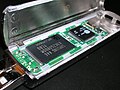
The PSP's eDRAM memory chip is the earliest known use of a three-dimensional integrated circuit (3D IC) chip in a commercial product. The eDRAM (embedded...
16 KB (2,157 words) - 23:09, 12 July 2024
Kryder's law Volatile RAM Hardware cache CPU cache Scratchpad memory DRAM eDRAM SDRAM SGRAM LPDDR QDRSRAM EDO DRAM XDR DRAM RDRAM DDR GDDR HBM SRAM 1T-SRAM...
185 KB (16,890 words) - 03:51, 7 July 2024
SDRAM @ 200 MHz 6.4 GB/s 512 MB of GDDR3 RAM @ 700 MHz 22.4 GB/s, 10 MB EDRAM GPU frame buffer memory 8 GB of DDR3 RAM @ 2133 MHz 68.3 GB/s, 32 MB ESRAM...
100 KB (7,902 words) - 19:44, 22 July 2024

GPU, the world's first GPU utilizing HBM3 on March 22, 2022. Stacked DRAM eDRAM Chip stack multi-chip module Hybrid Memory Cube (HMC): stacked memory standard...
34 KB (3,513 words) - 13:37, 20 July 2024

Iris Pro graphics with Direct3D feature level 12_1 with up to 128 MB of L4 eDRAM cache on certain SKUs. The Skylake line of processors retires VGA support...
95 KB (4,719 words) - 16:44, 5 July 2024

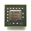
Retrieved March 31, 2020. "Apple (Samsung S5L8900) applications processor with eDRAM". SUBM TechInsights. Archived from the original on July 15, 2010. Retrieved...
44 KB (3,692 words) - 13:49, 23 July 2024