
Epitaxy (prefix epi- means "on top of”) refers to a type of crystal growth or material deposition in which new crystalline layers are formed with one...
30 KB (3,624 words) - 13:03, 8 December 2024

Molecular-beam epitaxy (MBE) is an epitaxy method for thin-film deposition of single crystals. MBE is widely used in the manufacture of semiconductor...
14 KB (1,469 words) - 09:52, 26 November 2024

Metalorganic vapour-phase epitaxy (MOVPE), also known as organometallic vapour-phase epitaxy (OMVPE) or metalorganic chemical vapour deposition (MOCVD)...
12 KB (1,318 words) - 21:22, 22 December 2024
fabrication plants. ASM's technologies include atomic layer deposition, epitaxy, chemical vapor deposition and diffusion. The company was founded by Arthur...
18 KB (1,786 words) - 20:34, 13 December 2024
Hydride vapour-phase epitaxy (HVPE) is an epitaxial growth technique often employed to produce semiconductors such as GaN, GaAs, InP and their related...
3 KB (409 words) - 21:22, 22 December 2024
Atomic layer epitaxy (ALE), more generally known as atomic layer deposition (ALD), is a specialized form of thin film growth (epitaxy) that typically deposit...
5 KB (568 words) - 18:07, 5 May 2021
Chemical beam epitaxy (CBE) forms an important class of deposition techniques for semiconductor layer systems, especially III-V semiconductor systems...
12 KB (1,661 words) - 21:22, 22 December 2024
epiwafer) is a wafer of semiconducting material made by epitaxial growth (epitaxy) for use in photonics, microelectronics, spintronics, or photovoltaics...
12 KB (1,262 words) - 01:54, 9 December 2024
The Center for Advanced Materials, formerly the Space Vacuum Epitaxy Center, is a laboratory established in 1986 at the University of Houston for researching...
2 KB (123 words) - 03:19, 22 February 2025

Epitaxy refers to a type of crystal growth or material deposition in which new crystalline layers are formed with one or more well-defined orientations...
19 KB (2,034 words) - 13:09, 16 February 2025

high-brightness LEDs used a thin film of GaN deposited via metalorganic vapour-phase epitaxy (MOVPE) on sapphire. Other substrates used are zinc oxide, with lattice...
40 KB (3,877 words) - 05:11, 29 January 2025

Shuttle. These flights proved the vacuum wake concept and realized the space epitaxy concept by growing the first-ever crystalline semiconductor thin films...
6 KB (674 words) - 20:41, 16 September 2023

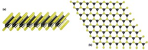
and perfect surface. The van der Waals interactions in epitaxy also known as van der Waals epitaxy (VDWE), is a phenomenon governed by weak van der Waals...
62 KB (6,989 words) - 17:44, 23 November 2024

Thermal laser epitaxy (TLE) is a physical vapor deposition technique that utilizes irradiation from continuous-wave lasers to heat sources locally for...
14 KB (1,534 words) - 11:48, 24 February 2025
from hydrogen. Hydrogen purifiers are used in metalorganic vapour phase epitaxy reactors for LED production. Fuel cell electric vehicles commonly use polymer...
16 KB (1,392 words) - 17:12, 14 November 2024
known as a pioneer of molecular beam epitaxy. Together with Alfred Y. Cho, Arthur pioneered molecular beam epitaxy at Bell Laboratories, where he published...
1 KB (157 words) - 12:54, 22 June 2024
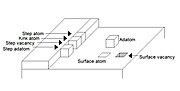
opposite of a surface vacancy. This term is used in surface chemistry and epitaxy, when describing single atoms lying on surfaces and surface roughness....
14 KB (2,253 words) - 14:13, 3 February 2025
devices after synthesizing the constituent material via molecular-beam epitaxy. She is a recipient of the Presidential Young Investigator Award from the...
10 KB (894 words) - 06:57, 16 November 2024
include: Molecular-beam epitaxy (MBE) Hydride vapor-phase epitaxy (HVPE) Liquid phase epitaxy (LPE) Metal-organic molecular-beam epitaxy (MOMBE) Atomic layer...
54 KB (2,525 words) - 04:36, 25 January 2025
African academic prizes. He is sometimes referred to as the "Father of Epitaxy". His research is seen as fundamental to applications in communication...
13 KB (1,380 words) - 23:40, 3 February 2025

Bridgman–Stockbarger method Van Arkel–de Boer process Czochralski method Epitaxy Flux method Fractional crystallization Fractional freezing Hydrothermal synthesis...
10 KB (1,237 words) - 01:45, 8 February 2025
development of the field-effect transistor. In 1960 Ross and others invented epitaxy. He subsequently rose through managerial ranks, ultimately serving as the...
5 KB (430 words) - 06:42, 20 February 2025
D. K; Gupta, G (2022). "van der Waals Epitaxy of Transition Metal Dichalcogenides via Molecular Beam Epitaxy: Looking Back and Moving Forward". Materials...
95 KB (10,532 words) - 03:01, 17 February 2025
zinc blende and wurtzite structures can be prepared by molecular beam epitaxy. The chemical properties of MgS resemble those of related ionic sulfides...
6 KB (519 words) - 14:28, 18 October 2024
Alcatel-Lucent's Bell Labs. He is known as the "father of molecular beam epitaxy"; a technique he developed at that facility in the late 1960s. He is also...
7 KB (638 words) - 06:57, 16 November 2024
on molecular-beam epitaxy (MBE), which is now an annual conference known as NAMBE (North American Conference on Molecular Beam Epitaxy). "IEEE James H....
4 KB (208 words) - 03:12, 31 July 2024
Bridgman–Stockbarger method Van Arkel–de Boer process Czochralski method Epitaxy Flux method Fractional crystallization Fractional freezing Hydrothermal synthesis...
3 KB (292 words) - 08:44, 24 October 2023

different substances to produce layered, crystalline films. See Atomic layer epitaxy. Combustion chemical vapor deposition (CCVD) – Combustion Chemical Vapor...
42 KB (5,009 words) - 19:14, 8 January 2025