
Molecular-beam epitaxy (MBE) is an epitaxy method for thin-film deposition of single crystals. MBE is widely used in the manufacture of semiconductor devices...
14 KB (1,532 words) - 09:31, 29 June 2024

by molecular beam epitaxy and their properties," Thin Solid Films, vol. 100, pp. 291–317, 1983. Cheng, K. Y. (November 1997). "Molecular beam epitaxy technology...
30 KB (3,602 words) - 11:26, 24 April 2024
Chemical beam epitaxy (CBE) forms an important class of deposition techniques for semiconductor layer systems, especially III-V semiconductor systems....
12 KB (1,661 words) - 16:11, 15 February 2024

create complex semiconductor multilayer structures. In contrast to molecular-beam epitaxy (MBE), the growth of crystals is by chemical reaction and not physical...
12 KB (1,318 words) - 07:09, 23 February 2024

Gallium nitride (section Molecular beam epitaxy)
molecular beam epitaxy or metalorganic vapour phase epitaxy. This process can be further modified to reduce dislocation densities. First, an ion beam...
38 KB (3,738 words) - 14:02, 11 July 2024
D. K; Gupta, G (2022). "van der Waals Epitaxy of Transition Metal Dichalcogenides via Molecular Beam Epitaxy: Looking Back and Moving Forward". Materials...
93 KB (10,303 words) - 03:10, 15 July 2024
collisions between the particles. Molecular beams are useful for fabricating thin films in molecular beam epitaxy and artificial structures such as quantum...
8 KB (884 words) - 00:01, 23 March 2024
Research at Alcatel-Lucent's Bell Labs. He is known as the "father of molecular beam epitaxy"; a technique he developed at that facility in the late 1960s. He...
7 KB (638 words) - 05:25, 18 August 2023
gap allows for the creation of desirable electrical properties. Molecular-beam epitaxy is a technique used to construct thin epitaxial films of materials...
7 KB (873 words) - 08:47, 24 October 2023

Artists Community complex. In 1968, molecular beam epitaxy was developed by J.R. Arthur and A.Y. Cho; molecular beam epitaxy allows semiconductor chips and...
151 KB (12,795 words) - 15:29, 1 July 2024

where they can absorb, nucleate, and grow on a desired substrate. Molecular beam epitaxy (MBE) has been used since 2000 to create high-quality semiconductor...
18 KB (2,477 words) - 12:13, 3 July 2024
perovskites, using techniques such as pulsed laser deposition and molecular-beam epitaxy. These films can be a couple of nanometres thick or as small as...
48 KB (4,995 words) - 02:47, 10 July 2024
photolithography, ion beam etch and deposition, metal organic chemical vapor deposition (MOCVD), wet wafer processing, molecular beam epitaxy (MBE), atomic layer...
19 KB (1,923 words) - 12:43, 13 July 2024

the alloy AlxGa1−xAs can be grown using molecular-beam epitaxy (MBE) or using metalorganic vapor-phase epitaxy (MOVPE). Because GaAs and AlAs have almost...
46 KB (5,183 words) - 09:13, 2 May 2024
scientist best known as a pioneer of molecular beam epitaxy. Together with Alfred Y. Cho, Arthur pioneered molecular beam epitaxy at Bell Laboratories, where he...
1 KB (157 words) - 12:54, 22 June 2024

Molecular Beam Epitaxy Research Group. 2014-08-19. Retrieved 2019-08-14. Johnson, Shane (May 1998). "In situ temperature control of molecular beam epitaxy...
52 KB (6,298 words) - 19:03, 3 June 2024
evaporating material in Knudsen cells, they are commonly used in molecular-beam epitaxy. The Knudsen effusion cell was developed by Martin Knudsen (1871–1949)...
2 KB (210 words) - 20:01, 5 January 2023
workshop on molecular-beam epitaxy (MBE), which is now an annual conference known as NAMBE (North American Conference on Molecular Beam Epitaxy). "IEEE James...
4 KB (199 words) - 02:46, 4 July 2023
photonic devices after synthesizing the constituent material via molecular-beam epitaxy. She is a recipient of the Presidential Young Investigator Award...
10 KB (894 words) - 20:37, 16 May 2024
Andrade, Roberto (2019). "Local roughness exponent in the nonlinear molecular-beam-epitaxy universality class in one-dimension". Physical Review E. 99 (2):...
10 KB (873 words) - 00:22, 13 January 2024

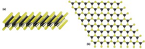
Tantalum diselenide (section Molecular Beam Epitaxy)
one opposed to others, as shown in the relative image. Through molecular beam epitaxy it is possible to grow one single trilayer of 2H-TaSe2, also known...
29 KB (3,291 words) - 02:42, 7 July 2024
news outlet covering the Middle East Migration enhanced epitaxy, a refined molecular-beam epitaxy technique Ministry of Ecology and Environment of the People's...
1 KB (178 words) - 02:51, 11 July 2024

emitting diodes with high internal quantum efficiency grown by molecular beam epitaxy". Applied Physics Letters. 98 (8): 081110. Bibcode:2011ApPhL..98h1110L...
166 KB (18,393 words) - 23:33, 17 July 2024

refractory metals, a process that is challenging to perform with molecular beam epitaxy. TLE uses continuous-wave lasers (typically with a wavelength of...
13 KB (1,373 words) - 06:18, 10 June 2024
interested in nanoscale engineering and imaging of materials, using molecular beam epitaxy and scanning probe microscopy. Hoffman has received several awards...
12 KB (954 words) - 22:41, 27 April 2024

suitable epitaxial deposition processes, including molecular-beam epitaxy and metal organic vapor-phase epitaxy. The design of the quantum wells can be engineered...
34 KB (3,594 words) - 05:06, 15 July 2024
of epiwafers manufactured by metalorganic vapour phase epitaxy (MOCVD), molecular beam epitaxy (MBE) and chemical vapor deposition (CVD).[citation needed]...
9 KB (874 words) - 15:01, 11 March 2024

sputter deposition; on a laboratory scale molecular beam epitaxy, pulsed laser deposition and electron beam physical vapor deposition are also utilized...
26 KB (3,271 words) - 01:38, 2 January 2024

layered materials with alternating compositions by techniques like molecular-beam epitaxy. These methods are exploited in the design of heterojunction bipolar...
23 KB (2,484 words) - 00:28, 11 June 2024