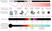
The nanometre (international spelling as used by the International Bureau of Weights and Measures; SI symbol: nm), or nanometer (American spelling), is...
5 KB (409 words) - 15:47, 30 May 2024
350 nm process (redirect from 350 nanometre)
The 350 nanometer process (350 nm process) is a level of semiconductor process technology that was reached in the 1995–1996 timeframe by leading semiconductor...
3 KB (208 words) - 05:23, 7 February 2024
800 nm process (redirect from 800 nanometre)
The 800 nm process (800 nanometer process) is a level of semiconductor process technology that was reached in the 1987–1990 timeframe, by companies, such...
2 KB (173 words) - 18:13, 1 June 2024
32 nm process (redirect from 32 nanometre)
"45 nm" process in CMOS (MOSFET) semiconductor device fabrication. "32-nanometre" refers to the average half-pitch (i.e., half the distance between identical...
12 KB (1,213 words) - 22:04, 25 April 2024
250 nm process (redirect from 250 nanometre)
The 250 nm process (250 nanometer process or 0.25 μm process) is a level of semiconductor process technology that was reached by most manufacturers in...
1 KB (102 words) - 02:29, 11 February 2024
180 nm process (redirect from 180 nanometre)
The 180 nm process is a MOSFET (CMOS) semiconductor process technology that was commercialized around the 1998–2000 timeframe by leading semiconductor...
4 KB (350 words) - 01:50, 1 December 2023
22 nm process (redirect from 22 nanometre)
possibly disturbing Moore's law. The 20-nanometre node is an intermediate half-node die shrink based on the 22-nanometre process. TSMC began mass production...
8 KB (801 words) - 00:51, 28 February 2024
2 nm process (redirect from 2 nanometre process)
In semiconductor manufacturing, the "2 nm process" is the next MOSFET (metal–oxide–semiconductor field-effect transistor) die shrink after the "3 nm" process...
29 KB (2,375 words) - 01:36, 15 June 2024
14 nm process (redirect from 14 nanometre)
December 2007, Toshiba demonstrated a prototype memory unit that used 15-nanometre thin lines. In December 2009, National Nano Device Laboratories, owned...
31 KB (2,719 words) - 15:24, 5 July 2024
65 nm process (redirect from 65 nanometre)
The 65 nm process is an advanced lithographic node used in volume CMOS (MOSFET) semiconductor fabrication. Printed linewidths (i.e. transistor gate lengths)...
8 KB (808 words) - 00:53, 28 February 2024

ten-billionth (US) of a metre, a hundred-millionth of a centimetre, 0.1 nanometre, or 100 picometres. Its symbol is Å, a letter of the Swedish alphabet...
19 KB (2,036 words) - 05:13, 11 June 2024
45 nm process (redirect from 45 nanometre)
Per the International Technology Roadmap for Semiconductors, the 45 nm process is a MOSFET technology node referring to the average half-pitch of a memory...
14 KB (1,395 words) - 00:52, 28 February 2024
130 nm process (redirect from 130 nanometre)
The 130 nanometer (130 nm) process is a level of semiconductor process technology that was reached in the 2000–2001 timeframe by such leading semiconductor...
3 KB (267 words) - 15:14, 11 January 2024

Die of a PIC12C508 8-bit, fully static, EEPROM/EPROM/ROM-based CMOS microcontroller manufactured by Microchip Technology using a 1200 nanometre process...
60 KB (7,609 words) - 03:26, 30 April 2024

Coast Pilots and Sailing Directions. It conflicts with the SI symbol for nanometre. The word mile is from the Latin phrase for a thousand paces: mille passus...
20 KB (2,008 words) - 17:42, 29 June 2024

not change irrespective of the prefix (as in centimetre, millimetre, nanometre and so on). It is generally preferred by the British Broadcasting Corporation...
12 KB (1,082 words) - 16:13, 20 March 2024
600 nm process (redirect from 600 nanometre)
The 600 nanometer process (600 nm process) is a level of semiconductor process technology that was reached in the 1994–1995 timeframe, by most leading...
1 KB (86 words) - 18:24, 21 October 2023

with process nodes from 2 microns to 3 nanometres. TSMC was the first foundry to market 7-nanometre and 5-nanometre (used by the 2020 Apple A14 and M1 SoCs...
94 KB (7,315 words) - 19:53, 10 July 2024
90 nm process (redirect from 90 nanometre)
The 90 nm process refers to the technology used in semiconductor manufacturing to create integrated circuits with a minimum feature size of 90 nanometers...
9 KB (867 words) - 00:53, 28 February 2024

suspension). The dispersed phase particles have a diameter of approximately 1 nanometre to 1 micrometre. Some colloids are translucent because of the Tyndall...
42 KB (4,865 words) - 04:01, 5 July 2024

opposite violet. It has a dominant wavelength of approximately 625–740 nanometres. It is a primary color in the RGB color model and a secondary color (made...
110 KB (12,246 words) - 18:46, 19 June 2024

length. The picometre is one thousand femtometres, one thousandth of a nanometre (1/1000 nm), one millionth of a micrometre (also known as a micron)...
3 KB (284 words) - 04:42, 16 May 2024

001 mm, or about 0.00004 inch). The nearest smaller common SI unit is the nanometre, equivalent to one thousandth of a micrometre, one millionth of a millimetre...
10 KB (937 words) - 09:51, 2 July 2024

Mm2 10−12 square micrometre μm2 1018 square gigametre Gm2 10−18 square nanometre nm2 1024 square terametre Tm2 10−24 square picometre pm2 1030 square petametre...
5 KB (309 words) - 05:06, 2 April 2024
10 nm process (redirect from 10 nanometre)
In semiconductor fabrication, the International Technology Roadmap for Semiconductors (ITRS) defines the "10 nanometer process" as the MOSFET technology...
21 KB (1,938 words) - 22:33, 6 June 2024
of- Two television cameras operating in visible (600 nanometre) and near-infrared (800 nanometre) and collected data related to hydrology, forestry and...
5 KB (278 words) - 03:04, 6 February 2024

a centimetre. One millimetre is equal to 1000 micrometres or 1000000 nanometres. Since an inch is officially defined as exactly 25.4 millimetres, a millimetre...
6 KB (471 words) - 01:34, 6 June 2024

soft X-ray flux within the wavelength bands 0.05 to 0.4 and 0.1 to 0.8 nanometres (0.5 to 4 and 1 to 8 ångströms) measured by the GOES spacecraft in geosynchronous...
47 KB (4,981 words) - 17:01, 12 July 2024

have been studied are spherical and have a diameter between 20 and 300 nanometres. Some filoviruses, which are filaments, have a total length of up to 1400 nm;...
154 KB (18,238 words) - 13:18, 10 July 2024