
Epitaxy (prefix epi- means "on top of”) refers to a type of crystal growth or material deposition in which new crystalline layers are formed with one...
30 KB (3,602 words) - 11:26, 24 April 2024

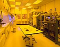
Molecular-beam epitaxy (MBE) is an epitaxy method for thin-film deposition of single crystals. MBE is widely used in the manufacture of semiconductor...
14 KB (1,532 words) - 09:31, 29 June 2024

Metalorganic vapour-phase epitaxy (MOVPE), also known as organometallic vapour-phase epitaxy (OMVPE) or metalorganic chemical vapour deposition (MOCVD)...
12 KB (1,318 words) - 07:09, 23 February 2024
Hydride vapour-phase epitaxy (HVPE) is an epitaxial growth technique often employed to produce semiconductors such as GaN, GaAs, InP and their related...
3 KB (409 words) - 19:52, 5 February 2024
Atomic layer epitaxy (ALE), more generally known as atomic layer deposition (ALD), is a specialized form of thin film growth (epitaxy) that typically deposit...
5 KB (568 words) - 18:07, 5 May 2021

Thermal laser epitaxy (TLE) is a physical vapor deposition technique that utilizes irradiation from continuous-wave lasers to heat sources locally for...
13 KB (1,373 words) - 06:18, 10 June 2024
Chemical beam epitaxy (CBE) forms an important class of deposition techniques for semiconductor layer systems, especially III-V semiconductor systems...
12 KB (1,661 words) - 16:11, 15 February 2024
fabrication plants. ASM's technologies include atomic layer deposition, epitaxy, chemical vapor deposition and diffusion. The company was founded by Arthur...
18 KB (1,786 words) - 00:49, 4 April 2024
Bridgman–Stockbarger method Van Arkel–de Boer process Czochralski method Epitaxy Flux method Fractional crystallization Fractional freezing Hydrothermal synthesis...
3 KB (292 words) - 08:44, 24 October 2023
epiwafer) is a wafer of semiconducting material made by epitaxial growth (epitaxy) for use in photonics, microelectronics, spintronics, or photovoltaics...
11 KB (1,262 words) - 01:12, 22 July 2023
Selective area epitaxy is the local growth of epitaxial layer through a patterned amorphous dielectric mask (typically SiO2 or Si3N4) deposited on a semiconductor...
7 KB (907 words) - 16:10, 15 February 2024
(ALD) Physical vapor deposition (PVD) Sputtering Evaporation Epitaxy Molecular beam epitaxy (MBE) Ion beam deposition Plasma ashing (for complete photoresist...
105 KB (11,171 words) - 01:54, 20 July 2024

Bridgman–Stockbarger method Van Arkel–de Boer process Czochralski method Epitaxy Flux method Fractional crystallization Fractional freezing Hydrothermal synthesis...
12 KB (1,548 words) - 20:55, 4 January 2024

high-brightness LEDs used a thin film of GaN deposited via metalorganic vapour-phase epitaxy (MOVPE) on sapphire. Other substrates used are zinc oxide, with lattice...
38 KB (3,738 words) - 14:02, 11 July 2024

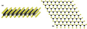
Graphene nanoribbon (section Epitaxy)
Graphene nanoribbons (GNRs, also called nano-graphene ribbons or nano-graphite ribbons) are strips of graphene with width less than 100 nm. Graphene ribbons...
44 KB (4,988 words) - 08:06, 26 June 2024
The Center for Advanced Materials, formerly the Space Vacuum Epitaxy Center, is a laboratory established in 1986 at the University of Houston for researching...
2 KB (123 words) - 05:30, 2 February 2024
include: Molecular-beam epitaxy (MBE) Hydride vapor-phase epitaxy (HVPE) Liquid phase epitaxy (LPE) Metal-organic molecular-beam epitaxy (MOMBE) Atomic layer...
54 KB (2,524 words) - 10:00, 26 June 2024
known as a pioneer of molecular beam epitaxy. Together with Alfred Y. Cho, Arthur pioneered molecular beam epitaxy at Bell Laboratories, where he published...
1 KB (157 words) - 12:54, 22 June 2024

Gd3Ga2(GaO4)3 which is synthesized for use as a substrate for liquid-phase epitaxy of magnetic garnet films for bubble memory and magneto-optical applications...
53 KB (5,142 words) - 23:35, 8 July 2024

satellite power applications, are made by molecular-beam epitaxy or metalorganic vapour-phase epitaxy of thin films of gallium arsenide, indium gallium phosphide...
74 KB (8,743 words) - 00:58, 13 June 2024
Graphene production techniques (section Epitaxy)
commonly referred to as epitaxy) or epitaxial layer deposition on a sapphire (Heteroepitaxy). A special method in CVD, called Epitaxy or Epitaxial Layer Deposition...
98 KB (10,670 words) - 10:08, 23 April 2024

Beam Epitaxy Research Group. 2014-08-19. Retrieved 2019-08-14. Johnson, Shane (May 1998). "In situ temperature control of molecular beam epitaxy growth...
52 KB (6,298 words) - 19:03, 3 June 2024

Community complex. In 1968, molecular beam epitaxy was developed by J.R. Arthur and A.Y. Cho; molecular beam epitaxy allows semiconductor chips and laser matrices...
151 KB (12,795 words) - 15:29, 1 July 2024
from hydrogen. Hydrogen purifiers are used in metalorganic vapour phase epitaxy reactors for LED production. Fuel cell electric vehicles commonly use polymer...
15 KB (1,353 words) - 01:09, 16 July 2024
allows for the creation of desirable electrical properties. Molecular-beam epitaxy is a technique used to construct thin epitaxial films of materials ranging...
7 KB (873 words) - 08:47, 24 October 2023

Vesborg, Peter C. K. (11 September 2023). "Laser-Annealing and Solid-Phase Epitaxy of Selenium Thin-Film Solar Cells". ACS Applied Energy Materials. 6 (17):...
96 KB (11,043 words) - 17:40, 30 June 2024
of epiwafers manufactured by metalorganic vapour phase epitaxy (MOCVD), molecular beam epitaxy (MBE) and chemical vapor deposition (CVD).[citation needed]...
9 KB (874 words) - 15:01, 11 March 2024
D. K; Gupta, G (2022). "van der Waals Epitaxy of Transition Metal Dichalcogenides via Molecular Beam Epitaxy: Looking Back and Moving Forward". Materials...
93 KB (10,303 words) - 03:10, 15 July 2024