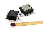
In semiconductor fabrication, a resist is a thin layer used to transfer a circuit pattern to the semiconductor substrate which it is deposited upon. A...
5 KB (607 words) - 20:41, 16 May 2024

Semiconductor device fabrication is the process used to manufacture semiconductor devices, typically integrated circuits (ICs) such as computer processors...
109 KB (11,593 words) - 16:33, 27 September 2024
(semiconductor fabrication), applied to semiconductor fabrication Resist (Kosheen album), or the title song Resist (Midnight Oil album), 2022 Resist (Within...
2 KB (320 words) - 07:53, 17 January 2024

In semiconductor production, doping is the intentional introduction of impurities into an intrinsic (undoped) semiconductor for the purpose of modulating...
35 KB (4,525 words) - 17:33, 6 September 2024

applications of the resist principle have recently developed in microelectronics and nanotechnology. An example is resists in semiconductor fabrication, using photoresists...
6 KB (735 words) - 03:45, 27 January 2024
MOSFET (redirect from Metal oxide semiconductor field-effect transistor)
advantages of the device, notably ease of fabrication and its application in integrated circuits. Usually the semiconductor of choice is silicon. Some chip manufacturers...
99 KB (11,949 words) - 02:40, 25 September 2024

CMOS (redirect from Complementary Metal Oxide Semiconductor)
metal–oxide–semiconductor (CMOS, pronounced "sea-moss", /siːmɑːs/, /-ɒs/) is a type of metal–oxide–semiconductor field-effect transistor (MOSFET) fabrication process...
57 KB (6,532 words) - 16:49, 26 September 2024

Photoresist (redirect from Negative resist)
A photoresist (also known simply as a resist) is a light-sensitive material used in several processes, such as photolithography and photoengraving, to...
29 KB (3,241 words) - 09:30, 11 August 2024
photoresist. Photolithography is the most common method for the semiconductor fabrication of integrated circuits ("ICs" or "chips"), such as solid-state...
58 KB (6,445 words) - 02:12, 12 September 2024

Sheet resistance (redirect from Area resistivity)
made by semiconductor doping, metal deposition, resistive paste printing, and glass coating. Examples of these processes are: doped semiconductor regions...
9 KB (1,250 words) - 07:12, 23 July 2024
Glossary of microelectronics manufacturing terms (redirect from Glossary of semiconductor device fabrication)
layers from the surface of a wafer during semiconductor device fabrication fab – a semiconductor fabrication plant fan-out wafer-level packaging – an extension...
14 KB (1,689 words) - 11:55, 18 October 2023

CHIPS and Science Act (redirect from Creating Helpful Incentives to Produce Semiconductors for America Act)
trained semiconductor engineers in the United States. In May 2022, Texas Instruments broke ground on new 300-mm semiconductor wafer fabrication plants...
129 KB (12,389 words) - 19:25, 27 September 2024

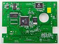
Integrated circuit (redirect from Semiconductor chip)
integration was made practical by technological advancements in semiconductor device fabrication. Since their origins in the 1960s, the size, speed, and capacity...
87 KB (9,261 words) - 08:32, 27 September 2024
Ultrapure water (category Semiconductor device fabrication)
for different users. The primary industries using UPW are: semiconductor devices fabrication process solar photovoltaics pharmaceuticals power generation...
64 KB (8,433 words) - 15:21, 24 September 2024

Integrated circuit packaging (redirect from Semiconductor packaging)
Integrated circuit packaging is the final stage of semiconductor device fabrication, in which the die is encapsulated in a supporting case that prevents...
15 KB (1,597 words) - 20:25, 22 April 2024

(named after Arthur Rock), which is that the capital cost of a semiconductor fabrication plant also increases exponentially over time. Numerous innovations...
104 KB (10,692 words) - 15:53, 25 September 2024

Quantum dot (redirect from Semiconductor nanocrystal)
techniques result in less expensive and less time-consuming methods of semiconductor fabrication. Quantum dots are usually coated with organic capping ligands...
113 KB (13,191 words) - 20:30, 10 September 2024

low throughput, limiting its usage to photomask fabrication, low-volume production of semiconductor devices, and research and development. Electron-beam...
38 KB (4,736 words) - 09:02, 10 July 2024
Spreading resistance profiling (category Semiconductor device fabrication)
analysis (SRA), is a technique used to analyze resistivity versus depth in semiconductors. Semiconductor devices depend on the distribution of carriers...
8 KB (1,090 words) - 17:11, 18 March 2024
Piezoresistive effect (redirect from Semiconductor gage)
The piezoresistive effect is a change in the electrical resistivity of a semiconductor or metal when mechanical strain is applied. In contrast to the piezoelectric...
15 KB (1,820 words) - 09:16, 28 May 2024
3 nm process (category International Technology Roadmap for Semiconductors lithography nodes)
late 2016, TSMC announced plans to construct a 5 nm–3 nm node semiconductor fabrication plant with a co-commitment investment of around US$15.7 billion...
44 KB (3,687 words) - 02:06, 25 September 2024
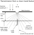
X-ray lithography is a process used in semiconductor device fabrication industry to selectively remove parts of a thin film of photoresist. It uses X-rays...
12 KB (1,623 words) - 17:49, 28 December 2022
Transfer length method (category Semiconductors)
technique used in semiconductor physics and engineering to determine the specific contact resistivity between a metal and a semiconductor. TLM has been developed...
28 KB (5,096 words) - 17:24, 26 September 2024
throughput, limiting single-column e-beams to photomask fabrication, low-volume production of semiconductor devices, and research and development. Multiple-electron...
16 KB (1,682 words) - 09:17, 28 May 2024
Printed circuit board (redirect from PCB fabrication)
innovations in the technology of printed electronic circuits and the fabrication of capacitors. This invention also represents a step in the development...
85 KB (10,823 words) - 15:47, 27 September 2024

cantilevers can deform over time. The fabrication of MEMS evolved from the process technology in semiconductor device fabrication, i.e. the basic techniques are...
45 KB (5,605 words) - 04:10, 21 September 2024
Chemical-mechanical polishing (category Semiconductor device fabrication)
etching and free abrasive polishing. It is used in the semiconductor industry to polish semiconductor wafers as part of the integrated circuit manufacturing...
9 KB (1,330 words) - 15:35, 19 September 2024
Hardmask (category Semiconductor device fabrication)
hardmask is a material used in semiconductor processing as an etch mask instead of a polymer or other organic "soft" resist material. Hardmasks are necessary...
3 KB (356 words) - 08:29, 16 July 2022

provide a high-resolution mask for fabrication of semiconductor devices. It is now mainly used in the fabrication of microfluidics (mainly via soft lithography...
14 KB (1,718 words) - 12:28, 6 September 2024

Epitaxy (category Semiconductor device fabrication)
nanotechnology and in semiconductor fabrication. Indeed, epitaxy is the only affordable method of high quality crystal growth for many semiconductor materials. In...
30 KB (3,600 words) - 22:11, 2 September 2024