The "32 nm" node is the step following the "45 nm" process in CMOS (MOSFET) semiconductor device fabrication. "32-nanometre" refers to the average half-pitch...
12 KB (1,213 words) - 22:04, 25 April 2024
graphics. L1 cache: 64 KB (32 KB data + 32 KB instructions) per core. L2 cache: 256 KB per core. Fabrication process: 45 nm. K-suffix processors have an...
469 KB (13,605 words) - 12:56, 25 July 2024
advancement over the previous 130 nm process. Eventually, it was succeeded by smaller process nodes, such as the 65 nm, 45 nm, and 32 nm processes. It was commercialized...
10 KB (875 words) - 03:00, 31 July 2024
dielectrics. In 2006, Samsung developed a 40 nm process. The successors to 45 nm technology are 32 nm, 22 nm, and then 14 nm technologies. Matsushita Electric Industrial...
14 KB (1,395 words) - 00:52, 28 February 2024
The "22 nm" node is the process step following 32 nm in CMOS MOSFET semiconductor device fabrication. The typical half-pitch (i.e., half the distance between...
8 KB (801 words) - 00:51, 28 February 2024
The "28 nm" lithography process is a half-node semiconductor manufacturing process based on a die shrink of the "32 nm" lithography process. It appeared...
5 KB (447 words) - 01:57, 29 April 2024

(Allendale), G0 (Conroe) The E5000 series and E6000 series use the same 45 nm Wolfdale-3M core as the E7000 series Core 2s, which has 3 MB L2 cache natively...
101 KB (3,933 words) - 09:25, 25 July 2024
instructions, SSE4.2. Westmere: 32 nm shrink of the Nehalem microarchitecture with several new features. Sandy Bridge 32 nm microarchitecture, released January...
51 KB (2,933 words) - 12:54, 6 August 2024
XD bit (an NX bit implementation), Intel VT-x, Smart Cache. Contains 45 nm "Ironlake" GPU. All models support: MMX, SSE, SSE2, SSE3, SSSE3, SSE4.1, SSE4...
150 KB (4,443 words) - 21:10, 23 June 2024
AMD 10h (section Lynx (32 nm SOI, dual or quad-core))
graphics capability, such as the Lynx Athlon II and Sempron X2). Fabrication 32 nm on GlobalFoundries SOI process Socket FM1 Die size: 228 mm2, with 1.178 billion...
78 KB (5,570 words) - 04:24, 28 June 2024
Wireless Display. Integrated PowerVR G6400 GPU, memory controller supporting two 32-bit LPDDR3 channels up to 4 GB, USB 3.0 controller, eMMC 4.5 Paired with Intel...
86 KB (3,164 words) - 09:36, 25 July 2024
(microprocessor) Wii U CPU Toshiba produced commercial 32 Gb NAND flash memory chips with the 32 nm process in 2009. Intel Core i3 and i5 processors, released...
76 KB (6,003 words) - 18:26, 6 August 2024

(Pentium, Nehalem microarchitecture) – 32 nm process technology (manufacturing 7 Jan 2010) 2 physical cores/2 threads 32+32 KB L1 cache 256 KB L2 cache 3 MB...
178 KB (13,535 words) - 19:50, 30 July 2024
Flexibility For Leading 32- And 64-Bit Computing". Retrieved 2008-05-20. "AMD Introduces New Players to the High-Performance 32- and 64-Bit AMD Opteron...
89 KB (2,189 words) - 09:24, 25 July 2024
List of AMD mobile processors (section "Llano" (32 nm))
platform targeting the ultra-portable notebook market. It features the 40 nm AMD Ontario (a 9-watt AMD APU for netbooks and small form factor desktops...
89 KB (3,390 words) - 21:59, 8 May 2024
Extensions (AVX) instruction set extensions to Sandy Bridge, first released on 32 nm in January 2011. Time has also brought improved support for virtualization...
235 KB (8,586 words) - 08:13, 5 August 2024
Socket AM2+ for single-CPU servers in 2007. These CPUs are produced on a 65 nm manufacturing process and are similar to the Agena Phenom X4 CPUs. The Socket...
43 KB (4,916 words) - 10:56, 5 July 2024
update to their plans for Kittson: it would have the same LGA1248 socket and 32 nm process as Poulson, effectively halting any further development of Itanium...
27 KB (1,456 words) - 20:26, 15 April 2024
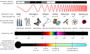
700 nm. The ångström, which is equal to 0.1 nm, was formerly used for these purposes. Since the late 1980s, in usages such as the 32 nm and the 22 nm semiconductor...
5 KB (409 words) - 15:47, 30 May 2024
series and features a 32 nm process (as it is based on the Westmere microarchitecture), integrated memory controller and 45 nm graphics controller and...
41 KB (2,671 words) - 08:23, 5 August 2024

Sandy Bridge is the codename for Intel's 32 nm microarchitecture used in the second generation of the Intel Core processors (Core i7, i5, i3). The Sandy...
58 KB (2,686 words) - 10:58, 21 May 2024
Athlon II is a family of AMD multi-core 45 nm central processing units, which is aimed at the budget to mid-range market and is a complementary product...
8 KB (663 words) - 14:36, 24 March 2024
Clarkdale Core i5 and Core i7 processors fabricated with a 32 nm process, down from a previous 45 nm process used in older iterations of the Nehalem processor...
7 KB (652 words) - 21:14, 10 May 2024
is comparable with scaled down (32 nm or less) planar NAND flash. However, with planar NAND scaling stopping at 16 nm, the cost per bit reduction can...
185 KB (16,909 words) - 12:05, 8 August 2024
Consumer Ultra-Low Voltage (section Celeron (32 nm))
processors come from the Intel Core product lines, and are based on a 10 nm process. List of AMD mobile microprocessors List of Intel Celeron microprocessors...
42 KB (371 words) - 11:54, 4 April 2024
originally designed in 45 nm complementary metal–oxide–semiconductor (CMOS) technology and subsequent models, codenamed Cedar, used a 32 nm process. The first...
41 KB (3,195 words) - 08:15, 5 August 2024
MOSFETs in 84 exposed fields (dies) on a wafer, manufactured using TSMC's 7 nm FinFET process. As of 2024[update], the GPU with the highest transistor count...
229 KB (10,140 words) - 05:13, 31 July 2024

from previous decades. Process sizes decreased about fourfold, from 180 nm to 45 nm. A new trend appears, the multi-chip module made of several chiplets...
52 KB (2,641 words) - 04:24, 31 July 2024
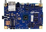
Intel Quark (section "Lakemont" (32 nm))
(P54C/i586) CPU. The first product in the Quark line is the single-core 32 nm X1000 SoC with a clock rate of up to 400 MHz. The system includes several...
15 KB (1,032 words) - 18:32, 26 June 2024

Apple silicon (category 32-bit microprocessors)
the iPhone 4S is 800 MHz. Like the A4, the A5 process size is 45 nm. An updated 32 nm version of the A5 processor was used in the 3rd-generation Apple...
192 KB (12,698 words) - 04:10, 6 August 2024