
A fin field-effect transistor (FinFET) is a multigate device, a MOSFET (metal–oxide–semiconductor field-effect transistor) built on a substrate where...
22 KB (2,338 words) - 12:49, 22 August 2024

Field-effect transistor (redirect from FET (transistor))
slower in operation than FETs. Chemical field-effect transistor CMOS FET amplifier Field effect (semiconductor) FinFET FlowFET Multigate device Lilienfeld...
53 KB (6,396 words) - 03:10, 29 September 2024
Multigate device (redirect from GAA FET)
device, based on FinFET technology. In 2011, Rice University researchers Masoud Rostami and Kartik Mohanram demonstrated that FINFETs can have two electrically...
40 KB (4,186 words) - 15:04, 26 September 2024
with "F" suffixes are without iGPUs. Fabrication process: TSMC N5 FinFET (N6 FinFET for the I/O die). v t e Self identifies as "AMD Radeon Graphics"....
7 KB (6,173 words) - 06:21, 18 September 2024


(ULL) 20 nm 16 nm (options: FinFET (FF), FinFET Plus (FF+), FinFET Compact (FFC) 12 nm (options: FinFET Compact (FFC), FinFET Nvidia (FFN)), enhanced version...
94 KB (7,483 words) - 14:09, 4 October 2024
of multi-gate MOSFET technology, while TSMC's 3nm process still uses FinFET (fin field-effect transistor) technology, despite TSMC developing GAAFET transistors...
44 KB (3,687 words) - 12:27, 11 October 2024
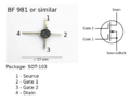
Transistor (section Field-effect transistor (FET))
transistor (MuGFET) Fin field-effect transistor (FinFET), source/drain region shapes fins on the silicon surface GAAFET, Similar to FinFET but nanowires are...
100 KB (10,419 words) - 11:29, 11 October 2024

SoC; it is manufactured by Samsung on their 14 nm FinFET LPE process and by TSMC on their 16 nm FinFET process. It was subsequently included in the first-generation...
197 KB (12,872 words) - 12:53, 8 October 2024
FinFET design. The GAAFET transistors used had 3 nanosheets stacked on top of each other, covered in their entirety by the same gate, just like FinFETs...
34 KB (2,874 words) - 18:15, 3 October 2024

Katherine (April 20, 2017). "Will Self-Heating Stop FinFETs". Semiconductor Engineering. "FinFET". "Foundries Rush 3-D Transistors - IEEE Spectrum". Bohr...
110 KB (11,589 words) - 17:06, 6 October 2024
semiconductor market in China. In 2016 GlobalFoundries licensed the 14 nm 14LPP FinFET process from Samsung Electronics. In 2018 GlobalFoundries developed the...
81 KB (5,276 words) - 01:41, 27 August 2024
following "22 nm" was expected to be "16 nm". All "14 nm" nodes use FinFET (fin field-effect transistor) technology, a type of multi-gate MOSFET technology...
32 KB (2,767 words) - 20:03, 25 August 2024
with "F" suffixes are without iGPUs. Fabrication process: TSMC N5 FinFET (N6 FinFET for the I/O die). v t e Self identifies as "AMD Radeon Graphics"....
29 KB (4,221 words) - 20:40, 7 October 2024

10, respectively. The architecture incorporates either 16 nm FinFET (TSMC) or 14 nm FinFET (Samsung) technologies. Initially, chips were only produced...
58 KB (3,333 words) - 09:17, 2 September 2024
have been their first to move from FinFET to Gate-All-Around transistors (GAAFET); Intel's version was named 'RibbonFET'. Their 2021 roadmap scheduled the...
30 KB (2,512 words) - 03:21, 28 September 2024
2022-01-02. Shilov, Anton. "SMIC Begins Volume Production of 14 nm FinFET Chips: China's First FinFET Line". www.anandtech.com. Archived from the original on 2019-11-15...
38 KB (2,942 words) - 01:33, 1 October 2024
Technologies. 1.92T FP16 OPS. Kirin 980 is HiSilicon's first SoC based on 7 nm FinFET technology. Interconnect: ARM Mali G76-MP10, Storage: UFS 2.1, Sensor Hub:...
68 KB (3,995 words) - 17:22, 20 September 2024
compiler. GCN graphics chips were fabricated with CMOS at 28 nm, and with FinFET at 14 nm (by Samsung Electronics and GlobalFoundries) and 7 nm (by TSMC)...
53 KB (4,452 words) - 22:36, 6 September 2024
International Technology Roadmap for Semiconductors (ITRS). It is based on FinFET (fin field-effect transistor) technology, a type of multi-gate MOSFET technology...
51 KB (4,729 words) - 14:07, 29 September 2024
respectively. Pascal was manufactured using TSMC's 16 nm FinFET process, and later Samsung's 14 nm FinFET process. The architecture is named after the 17th century...
23 KB (1,935 words) - 05:00, 24 July 2024
generation architecture, codenamed Vega, and are manufactured on 14 nm FinFET technology, developed by Samsung Electronics and licensed to GlobalFoundries...
14 KB (3,728 words) - 14:05, 8 February 2024
in 84 exposed fields (dies) on a wafer, manufactured using TSMC's 7 nm FinFET process. As of 2024[update], the GPU with the highest transistor count is...
229 KB (10,130 words) - 14:09, 28 September 2024
GF 14LPP (FinFET bulk) GF 12LP (FinFET bulk) TSMC N7 (FinFET bulk) TSMC N6 (FinFET bulk) CCD: TSMC N5 (FinFET bulk) cIOD: TSMC N6 (FinFET bulk) TSMC...
50 KB (4,734 words) - 22:56, 21 September 2024

take the form of multi-gate MOSFETs, with the FinFET being the most common nanoscale transistor. The FinFET has gate dielectric on three sides of the channel...
104 KB (10,696 words) - 21:24, 10 October 2024
20 nm nodes in 2014. The 22 nm process was superseded by commercial 14 nm FinFET technology in 2014. On August 18, 2008, AMD, Freescale, IBM, STMicroelectronics...
8 KB (801 words) - 00:51, 28 February 2024

instruction) per core. L2 cache: 1 MB per core. Fabrication process: TSMC N4 FinFET (N6 FinFET for the I/O die). v t e Manufacturer suggested retail price at launch...
27 KB (2,703 words) - 10:07, 9 October 2024

on a 14 nm FinFET process, developed by Samsung Electronics and licensed to GlobalFoundries. Polaris 30 chips are produced on a 12 nm FinFET process, developed...
7 KB (814 words) - 06:57, 21 July 2024
Tegra X1 (Nintendo Switch and Nvidia Shield TV) TSMC first began 16 nm FinFET chip production in 2013. Nvidia Tegra X1+ (later Nintendo Switch and Nvidia...
76 KB (6,003 words) - 18:26, 6 August 2024

The launch occurred on July 7, 2019. It is manufactured using TSMC's 7 nm FinFET semiconductor fabrication process. The Navi GPUs are the first AMD GPUs...
17 KB (1,624 words) - 18:44, 26 March 2024