Photolithography (also known as optical lithography) is a process used in the manufacturing of integrated circuits. It involves using light to transfer...
58 KB (6,445 words) - 02:12, 12 September 2024

Photolithography is a process in removing select portions of thin films used in microfabrication. Microfabrication is the production of parts on the micro-...
14 KB (1,648 words) - 07:27, 24 July 2023

in 1984. ASML specializes in the development and manufacturing of photolithography machines which are used to produce computer chips. As of 2023[update]...
42 KB (3,456 words) - 20:48, 19 October 2024

Ultraviolet (section Photolithography)
need for costly vacuum chambers. Significant examples include 193-nm photolithography equipment (for semiconductor manufacturing) and circular dichroism...
117 KB (12,618 words) - 22:04, 8 October 2024
the resolution attainable through photolithography. Computational lithography came to the forefront of photolithography technologies in 2008 when the semiconductor...
13 KB (1,504 words) - 21:30, 14 June 2023

shine through in a defined pattern. Photomasks are commonly used in photolithography for the production of integrated circuits (ICs or "chips") to produce...
20 KB (2,323 words) - 15:35, 24 August 2024

created by a photographic process, a method that may be referred to as "photolithography" (although the term usually refers to a vaguely similar microelectronics...
23 KB (2,890 words) - 22:49, 16 September 2024
Argon fluoride laser (section Photolithography)
range. ArF (and KrF) excimer lasers are widely used in high-resolution photolithography machines, a critical technology for microelectronic chip manufacturing...
10 KB (1,103 words) - 21:59, 29 July 2024

(EGS) or other semiconductor (such as GaAs) through processes such as photolithography. The wafer is cut (diced) into many pieces, each containing one copy...
5 KB (462 words) - 22:21, 18 August 2024
ASML may refer to: ASML Holding, a Dutch company that supplies photolithography systems for the semiconductor industry Atlanta, Stone Mountain and Lithonia...
441 bytes (95 words) - 21:54, 3 April 2024

film. It is employed in many fields of science, manufacturing (e.g., photolithography), and business, as well as its more direct uses for art, film and video...
84 KB (9,303 words) - 20:05, 30 September 2024

resist) is a light-sensitive material used in several processes, such as photolithography and photoengraving, to form a patterned coating on a surface. This...
29 KB (3,241 words) - 09:30, 11 August 2024

because the chips, with all their components, are printed as a unit by photolithography rather than being constructed one transistor at a time. Furthermore...
87 KB (9,261 words) - 18:01, 15 October 2024

Excimer laser (section Photolithography)
the 1960s, excimer lasers have been widely used in high-resolution photolithography machines, one of the critical technologies required for microelectronic...
21 KB (2,724 words) - 20:09, 25 August 2024

free-space optical communication, semiconducting chip manufacturing (photolithography), laser surgery and skin treatments, cutting and welding materials...
113 KB (12,669 words) - 20:51, 10 October 2024

integrated circuits (ICs). It is an essential part of the process of photolithography, which creates millions of microscopic circuit elements on the surface...
23 KB (3,207 words) - 03:37, 14 March 2024

Potential infrastructure for future technologies includes DNA origami on photolithography and quantum antennae for transferring information between ion traps...
51 KB (5,368 words) - 02:19, 20 October 2024
Optical proximity correction (OPC) is a photolithography enhancement technique commonly used to compensate for image errors due to diffraction or process...
16 KB (1,849 words) - 23:46, 21 July 2024

13.5 nm extreme ultraviolet light is used commercially for photolithography as part of the semiconductor fabrication process. This image shows an early...
13 KB (1,518 words) - 03:52, 22 September 2024

size, rather than using the latest EUV photolithography technology. SMEE's SSA800 machine lags photolithography industry leader ASML Holding in time: ASML...
9 KB (916 words) - 01:49, 7 September 2024

which the light travels. The lenses in the highest resolution "dry" photolithography scanners focus light in a cone whose boundary is nearly parallel to...
10 KB (1,089 words) - 18:17, 16 October 2024

then thinly sliced to form a wafer substrate. The planar process of photolithography then integrates unipolar transistors, capacitors, diodes, and resistors...
127 KB (13,304 words) - 02:26, 12 October 2024

prints the desired circuit pattern onto the silicon wafer bypassing photolithography and can produce circuits equivalent to 5 nm scale. Canon's products...
50 KB (4,542 words) - 06:20, 30 August 2024
imaging systems, spectroscopy, telescopes, and excimer lasers (used for photolithography in the form of a fused lens). It is transparent over a broad range...
10 KB (843 words) - 21:21, 6 October 2024
"next generation" have entered commercial production, and open-air photolithography, with visible light projected through hand-drawn photomasks, has gradually...
10 KB (1,111 words) - 00:58, 10 January 2024
Nanolithography (section Photolithography)
skyrocketed. Photolithography was applied to these structures for the first time in 1958 beginning the age of nanolithography. Since then, photolithography has...
15 KB (1,679 words) - 11:06, 19 October 2024

Gas mixtures that include high-purity neon are used in lasers for photolithography in semiconductor device fabrication. Liquefied neon is commercially...
32 KB (3,829 words) - 07:05, 19 October 2024

Anti-reflective coating (section Photolithography)
lenses. Antireflective coatings (ARC) are often used in microelectronic photolithography to help reduce image distortions associated with reflections off the...
34 KB (4,063 words) - 12:26, 1 October 2024
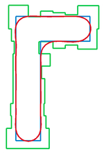
measurement is known as the linewidth. Patterning often refers to photolithography which allows a device design or pattern to be defined on the device...
109 KB (11,548 words) - 07:14, 16 October 2024

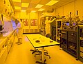
yellow light filter. These lamps are commonly used as lighting for photolithography work in cleanrooms and as "bug repellent" outdoor lighting (the efficacy...
96 KB (11,335 words) - 08:59, 5 October 2024