Computational lithography (also known as computational scaling) is the set of mathematical and algorithmic approaches designed to improve the resolution...
13 KB (1,502 words) - 13:32, 14 December 2024
Photolithography (redirect from Optical lithography)
Photolithography (also known as optical lithography) is a process used in the manufacturing of integrated circuits. It involves using light to transfer...
58 KB (6,471 words) - 13:25, 23 December 2024
self-assembly or aggressive cut reduction. Computational lithography Nanolithography Quantum Lithography Tallis, Anton Shilov, Billy. "Samsung Starts...
10 KB (1,111 words) - 13:20, 14 December 2024
company Ambios Technology, Inc. In 2014, the company acquired computational lithography and inspection company Luminescent Technologies, Inc. In 2017...
16 KB (1,439 words) - 11:47, 14 December 2024
Photomask (category Lithography (microfabrication))
other, at least one mask is required for each of these layers. Computational lithography Integrated circuit layout design protection (or "Mask work") Mask...
20 KB (2,323 words) - 15:35, 24 August 2024
548923. S2CID 110913847. Retrieved 19 October 2016. "Calibre Computational Lithography". Mentor Graphics. Archived from the original on 2016-05-31. Retrieved...
2 KB (189 words) - 18:26, 9 February 2022
In semiconductor device fabrication, the inverse lithography technology (ILT) is an approach to photomask design. This is basically an approach to solve...
2 KB (221 words) - 22:09, 10 November 2022
Optical proximity correction (category Lithography (microfabrication))
only approach the dense case, not match it. Computational lithography Phase-shift mask Inverse lithography Ronse, K. (1994). "Fundamental principles of...
16 KB (1,849 words) - 23:46, 21 July 2024
Moore's law (redirect from Computational power)
chips. The cost of the tools, principally EUVL (Extreme ultraviolet lithography), used to manufacture chips doubles every 4 years. Rising manufacturing...
104 KB (10,700 words) - 07:57, 23 December 2024
Computer-generated holography (redirect from Computational holography)
proposed in the fields of holographic information and computational reduction as well as in computational and quantization techniques. The algorithms can be...
21 KB (2,595 words) - 20:46, 31 May 2024
Mask shop (category Lithography (microfabrication))
increase and the product turn around time grow longer as well. Computational lithography GDSII Tracy, Dan; Deborah Geiger (April 14, 2014). "SEMI Reports...
4 KB (356 words) - 12:18, 22 December 2024
Biological computing (category Models of computation)
ultimately result in the computational functionality of a computer. Biocomputers use biologically derived materials to perform computational functions. A biocomputer...
18 KB (2,205 words) - 17:10, 16 December 2024
Nanotechnology (section Lithography)
techniques of lithography, such as optical lithography, X-ray lithography, dip pen lithography, electron beam lithography or nanoimprint lithography offer top-down...
69 KB (7,036 words) - 16:05, 14 November 2024
Patterned media (section Ion beam lithography)
be written on tracks with predetermined shapes, which are created by lithography (see below) on the disk. The trajectories that are required to be followed...
9 KB (1,103 words) - 10:40, 2 November 2024
Photo-optical Instrumentation Engineers (SPIE), for achievements in computational lithography, digital, biomedical, and electronic imaging. 2013 - Optical Society...
3 KB (271 words) - 15:42, 31 January 2024
Cost for processes such as lithography is proportional to wafer area, and larger wafers would not reduce the lithography contribution to die cost. Nikon...
37 KB (4,141 words) - 16:33, 22 November 2024
interferometric optical lithography. His research specializations include linear optical implementations of quantum communication and computation protocols, quantum...
6 KB (469 words) - 12:50, 22 October 2024
(stylized as cādence) is an American multinational technology and computational software company. Headquartered in San Jose, California, Cadence was...
62 KB (4,881 words) - 23:19, 23 December 2024
Stereolithography (redirect from Stereo lithography)
innovation in France. The term “stereolithography” (Greek: stereo-solid and lithography) was coined in 1984 by Chuck Hull when he filed his patent for the process...
24 KB (2,681 words) - 10:50, 2 November 2024
for dealing with effects of variation. Stricter design rules – Due to lithography and etch issues with scaling, design rule checking for layout has become...
14 KB (1,599 words) - 08:48, 3 December 2024
Retrieved 2022-05-30. "STL (STereoLithography) File Format Family". Library of Congress. Retrieved 2022-05-30. StereoLithography Interface Specification, 3D...
18 KB (2,129 words) - 04:05, 12 December 2024
Dot gain, or tonal value increase, is a phenomenon in offset lithography and some other forms of printing which causes printed material to look darker...
12 KB (1,674 words) - 23:59, 20 December 2024
Richard R. Freeman (section Lithography)
350 peer-reviewed research papers and holds 6 patents in the fields of lithography and laser processing. His graduate textbook, Electromagnetic Radiation...
16 KB (1,677 words) - 07:47, 22 October 2024
the two lowest eigenstates will serve as the computational basis for the logical qubit. Computational operations are performed by pulsing the qubit with...
16 KB (2,244 words) - 17:52, 4 December 2024
more sensitive resins/resists, two-photon absorption found its way into lithography. One of the most distinguishing features of two-photon absorption is...
43 KB (5,510 words) - 03:17, 18 December 2024
gating High-κ dielectric Next-generation lithography Extreme ultraviolet lithography Immersion lithography Strain engineering Very Large Scale Integration...
40 KB (4,186 words) - 15:03, 18 November 2024
content by icons Klecksography – art of making images from inkblots Lithography – planographic printing technique Photography – art, practice or occupation...
5 KB (584 words) - 23:47, 18 April 2024
a large piece of material to small pieces, by various means such as lithography, milling or thermal oxidation. A bottom-up approach synthesizes the nanowire...
59 KB (6,848 words) - 07:36, 24 October 2024
Facility Director Adam Schwartzberg and founded by Jeff Bokor. Advanced lithography and thin-film processing emphasizing integration with chemical and biological...
5 KB (508 words) - 13:39, 2 May 2024
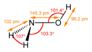
component in the "resist stripper", which removes photoresist after lithography. Hydroxylamine can also be used to better characterize the nature of...
27 KB (2,555 words) - 01:00, 17 December 2024


