Selective area epitaxy is the local growth of epitaxial layer through a patterned amorphous dielectric mask (typically SiO2 or Si3N4) deposited on a semiconductor...
7 KB (907 words) - 16:10, 15 February 2024

Epitaxy (prefix epi- means "on top of”) refers to a type of crystal growth or material deposition in which new crystalline layers are formed with one...
30 KB (3,604 words) - 10:44, 19 August 2024
devices including strained-layer indium gallium arsenide lasers and selective area epitaxy.[citation needed] Coleman is a Fellow of the IEEE and a member of...
9 KB (866 words) - 04:00, 31 July 2024
sae in Wiktionary, the free dictionary. SAE or Sae may refer to: Selective area epitaxy, local growth of epitaxial layer through a patterned dielectric...
3 KB (419 words) - 16:05, 15 July 2024
Chemical beam epitaxy (CBE) forms an important class of deposition techniques for semiconductor layer systems, especially III-V semiconductor systems...
12 KB (1,661 words) - 16:11, 15 February 2024

Toshiba has stopped research, possibly due to low yields. Some opt for epitaxy, which is difficult on silicon, while others, like the University of Cambridge...
166 KB (18,396 words) - 18:02, 31 July 2024
D. K; Gupta, G (2022). "van der Waals Epitaxy of Transition Metal Dichalcogenides via Molecular Beam Epitaxy: Looking Back and Moving Forward". Materials...
93 KB (10,303 words) - 07:22, 20 August 2024
Graphene production techniques (section Epitaxy)
commonly referred to as epitaxy) or epitaxial layer deposition on a sapphire (Heteroepitaxy). A special method in CVD, called Epitaxy or Epitaxial Layer Deposition...
98 KB (10,670 words) - 10:08, 23 April 2024

(ALD) Physical vapor deposition (PVD) Sputtering Evaporation Epitaxy Molecular beam epitaxy (MBE) Ion beam deposition Plasma ashing (for complete photoresist...
106 KB (11,198 words) - 14:06, 16 August 2024

Graphene nanoribbon (section Epitaxy)
additional active sites or modify the electronic structure, allowing for selective catalytic transformations. Science portal Technology portal Graphene oxide...
44 KB (4,988 words) - 08:06, 26 June 2024

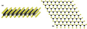
extraordinary electrical, thermal, and physical properties. It can be produced by epitaxy on an insulating or conducting substrate or by mechanical exfoliation (repeated...
48 KB (5,634 words) - 03:47, 27 July 2024
organometallic vapour phase epitaxy (OMVPE). Devices have been grown by molecular beam epitaxy (MBE) and liquid phase epitaxy (LPE). The internal quantum...
42 KB (5,566 words) - 22:34, 1 June 2024

and perfect surface. The van der Waals interactions in epitaxy also known as van der Waals epitaxy (VDWE), is a phenomenon governed by weak van der Waal's...
63 KB (6,985 words) - 06:27, 20 August 2024
Union by the team led by Nikolay Basov. In the early 1960s liquid phase epitaxy (LPE) was invented by Herbert Nelson of RCA Laboratories. By layering the...
51 KB (6,397 words) - 13:38, 6 August 2024

of semiconductor devices may involve the use of vapor-phase epitaxy. In vapor-phase epitaxy, a gas containing the dopant precursor can be introduced into...
35 KB (4,525 words) - 02:56, 21 June 2024
using a variety of methods such as molecular beam epitaxy (MBE) or metalorganic vapour phase epitaxy (MOVPE), also known as metalorganic chemical vapor...
35 KB (4,306 words) - 20:11, 1 May 2024

"Ga-assisted catalyst-free growth mechanism of Ga As nanowires by molecular beam epitaxy". Physical Review B. 77 (15): 155326. Bibcode:2008PhRvB..77o5326C. doi:10...
18 KB (1,554 words) - 17:22, 27 March 2024

gold-assisted vapor-liquid-solid (VLS) growth of GaAs nanowires by molecular beam epitaxy [1]. In 2008-2014, following Frank Glas [2], he developed theoretical approaches...
22 KB (2,425 words) - 14:24, 29 April 2023

high-power laser ablates material from the target into a vapor. Thermal laser epitaxy: a continuous-wave laser evaporates individual, free-standing elemental...
16 KB (1,868 words) - 09:54, 9 July 2024
can be produced by chemical vapor deposition, metalorganic vapour phase epitaxy, electrodeposition, pulsed laser deposition, sputtering, sol–gel synthesis...
73 KB (8,143 words) - 15:16, 19 August 2024

satellite power applications, are made by molecular-beam epitaxy or metalorganic vapour-phase epitaxy of thin films of gallium arsenide, indium gallium phosphide...
74 KB (8,761 words) - 13:06, 13 August 2024

GaN generated via Pt-assisted electroless etching of hydride vapor phase epitaxy GaN on sapphire". Journal of Applied Physics. 94 (12): 7526–7534. doi:10...
18 KB (2,228 words) - 22:38, 10 December 2023

Vesborg, Peter C. K. (11 September 2023). "Laser-Annealing and Solid-Phase Epitaxy of Selenium Thin-Film Solar Cells". ACS Applied Energy Materials. 6 (17):...
95 KB (11,044 words) - 22:05, 13 August 2024

of amorphous-crystalline silicon-heterojunctions on surfaces promoting epitaxy". Applied Physics Letters. 102 (12): 122106. Bibcode:2013ApPhL.102l2106M...
44 KB (4,936 words) - 12:41, 9 April 2024

occurs when a certain very small number of {110}<001> (Goss) grains grow selectively, about one in 106 primary grains, at the expense of many other primary...
20 KB (2,761 words) - 04:05, 15 July 2024
Li; Z Liu (2011). "Formation of bilayer Bernal graphene: layer-by-layer epitaxy via chemical vapor deposition". Nano Lett. 11 (3): 1106–10. Bibcode:2011NanoL...
23 KB (2,745 words) - 16:15, 5 February 2024
Solar cell (redirect from Wide area silicon)
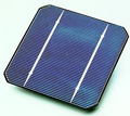
cell grown on top of another, typically using metalorganic vapour phase epitaxy. Each layer has a different band gap energy to allow it to absorb electromagnetic...
150 KB (17,048 words) - 18:24, 10 August 2024

spontaneously under certain conditions during molecular beam epitaxy (MBE) and metalorganic vapour-phase epitaxy (MOVPE), when a material is grown on a substrate...
113 KB (13,191 words) - 15:16, 19 August 2024
as a scaffold to support the photoactive heterojunction. Molecular beam epitaxy is used to deposit CdTe and CdS as the p/n-type materials and ion-assisted...
54 KB (7,332 words) - 20:53, 19 January 2024