14 nm process (redirect from 14 nanometer)
The "14 nanometer process" refers to a marketing term for the MOSFET technology node that is the successor to the "22 nm" (or "20 nm") node. The "14 nm"...
32 KB (2,767 words) - 20:03, 25 August 2024
3 nm process (redirect from 3 nanometer)
use of EUV lithography, and power and area improvement. The term "3 nanometer" has no direct relation to any actual physical feature (such as gate length...
44 KB (3,668 words) - 10:13, 15 September 2024
600 nm process (redirect from 600 nanometer)
The 600 nanometer process (600 nm process) is a level of semiconductor process technology that was reached in the 1994–1995 timeframe, by most leading...
1 KB (86 words) - 18:24, 21 October 2023
250 nm process (redirect from 250 nanometer)
The 250 nm process (250 nanometer process or 0.25 μm process) is a level of semiconductor process technology that was reached by most manufacturers in...
1 KB (102 words) - 02:29, 11 February 2024
2 nm process (redirect from 2 nanometer process)
field-effect transistor) die shrink after the 3 nm process node. The term "2 nanometer", or alternatively "20 angstrom" (a term used by Intel), has no relation...
30 KB (2,500 words) - 19:50, 13 September 2024
350 nm process (redirect from 350 nanometer)
The 350 nanometer process (350 nm process) is a level of semiconductor process technology that was reached in the 1995–1996 timeframe by leading semiconductor...
3 KB (208 words) - 05:23, 7 February 2024
800 nm process (redirect from 800 nanometer)
The 800 nm process (800 nanometer process) is a level of semiconductor process technology that was reached in the 1987–1990 timeframe, by companies, such...
2 KB (173 words) - 18:13, 1 June 2024
Chromatin (redirect from Nanometer fiber)
on a string structure (euchromatin). Multiple histones wrap into a 30-nanometer fiber consisting of nucleosome arrays in their most compact form (heterochromatin)...
53 KB (5,924 words) - 04:55, 20 August 2024
Die shrink (redirect from 40 nanometer)
The term die shrink (sometimes optical shrink or process shrink) refers to the scaling of metal–oxide–semiconductor (MOS) devices. The act of shrinking...
7 KB (652 words) - 21:14, 10 May 2024
130 nm process (redirect from 130 nanometer)
The 130 nanometer (130 nm) process is a level of semiconductor process technology that was reached in the 2000–2001 timeframe by such leading semiconductor...
3 KB (267 words) - 15:14, 11 January 2024
45 nm process (redirect from 45-nanometer)
Per the International Technology Roadmap for Semiconductors, the 45 nm process is a MOSFET technology node referring to the average half-pitch of a memory...
14 KB (1,395 words) - 00:52, 28 February 2024
Journal of Vacuum Science and Technology (redirect from Journal of Vacuum Science & Technology B: Microelectronics and Nanometer Structures)
1991–present Journal of Vacuum Science & Technology B: Microelectronics and Nanometer Structures Part A covers applied surface science, electronic materials...
4 KB (222 words) - 12:13, 12 September 2024
5 nm process (redirect from 5 nanometer)
as gate length, metal pitch or gate pitch) of the transistors is five nanometers in size. Historically, the number used in the name of a technology node...
34 KB (2,873 words) - 01:10, 10 September 2024
Three gold atoms lined up are about one nanometer (nm) long. If a toy marble were scaled down to one nanometer wide, Earth would scale to about 1 meter...
2 KB (453 words) - 11:03, 28 July 2024
65 nm process (redirect from 65-nanometer)
and Core i3-8121U Deep Dive Review". "Fujitsu Introduces World-class 65-Nanometer Process Technology for Advanced Server, Mobile Applications". Fujitsu...
8 KB (794 words) - 03:16, 12 August 2024
7 nm process (redirect from 7 nanometer)
process for 2024". Notebook Check. Morris, Kevin (July 23, 2020). "No More Nanometers: It's Time for New Node Naming". Electronic Engineering Journal. Retrieved...
51 KB (4,688 words) - 20:22, 15 September 2024
10 nm process (redirect from 10 nanometer)
International Technology Roadmap for Semiconductors (ITRS) defines the "10 nanometer process" as the MOSFET technology node following the "14 nm" node. Since...
21 KB (1,955 words) - 22:39, 6 September 2024
90 nm process (redirect from 90-nanometer)
manufacturing to create integrated circuits with a minimum feature size of 90 nanometers. It was an advancement over the previous 130 nm process. Eventually, it...
10 KB (875 words) - 03:00, 31 July 2024
a spectrum of ultraviolet light with wavelengths ranging from 290–320 nanometers. This spectrum is also commonly called the biological spectrum due to...
6 KB (894 words) - 12:37, 10 September 2024
32 nm process (redirect from 32-nanometer)
length, nor metal pitch, nor gate pitch on a "32nm" device is thirty-two nanometers. The "28 nm" node is an intermediate half-node die shrink based on the...
12 KB (1,213 words) - 22:04, 25 April 2024
180 nm process (redirect from 180 nanometer)
The 180 nm process is a MOSFET (CMOS) semiconductor process technology that was commercialized around the 1998–2000 timeframe by leading semiconductor...
4 KB (350 words) - 01:50, 1 December 2023
22 nm process (redirect from 22 nanometer)
gate length, metal pitch or gate pitch on a "22nm" device is twenty-two nanometers. The ITRS 2006 Front End Process Update indicates that equivalent physical...
8 KB (801 words) - 00:51, 28 February 2024

emit 280-330 nanometer, Fluorescent Narrow-Band that emit 312 nanometer, Excimer that emit 308 nanometer and LED that emit 290-300 nanometer. PUVA means...
4 KB (453 words) - 04:44, 4 October 2023

membrane filtration process that uses nanometer sized pores through which particles smaller than about 1–10 nanometers pass through the membrane. Nanofiltration...
24 KB (2,946 words) - 18:24, 8 August 2024
QSD8650A addition to the Snapdragon product suite, which was based on 45 nanometer manufacturing processes. It featured a 1.2 GHz processor and had lower...
75 KB (6,329 words) - 12:49, 26 August 2024

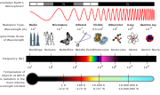
Orders of magnitude (length) (redirect from 1 nanometer)
The following are examples of orders of magnitude for different lengths. To help compare different orders of magnitude, the following list describes various...
181 KB (17,318 words) - 15:08, 12 September 2024
nano-optics is the study of the behavior of light on the nanometer scale, and of the interaction of nanometer-scale objects with light. It is a branch of optics...
24 KB (2,690 words) - 04:30, 31 July 2024
A nanofluid is a fluid containing nanometer-sized particles, called nanoparticles. These fluids are engineered colloidal suspensions of nanoparticles...
36 KB (3,996 words) - 04:30, 31 July 2024

microscopy (SPM), with demonstrated resolution on the order of fractions of a nanometer, more than 1000 times better than the optical diffraction limit. Atomic...
75 KB (9,806 words) - 04:32, 24 August 2024