Multigate device (redirect from 3D transistor)
(gate-all-around field-effect transistor), which are non-planar transistors, or 3D transistors. Multi-gate transistors are one of the several strategies...
40 KB (4,186 words) - 15:04, 26 September 2024

The field-effect transistor (FET) is a type of transistor that uses an electric field to control the flow of current in a semiconductor. It comes in two...
53 KB (6,396 words) - 03:10, 29 September 2024
semiconductor's transistor count to its die area. As of 2023[update], the highest transistor count in flash memory is Micron's 2 terabyte (3D-stacked) 16-die...
229 KB (10,130 words) - 14:09, 28 September 2024

metal–oxide–semiconductor) technology. FinFET is a type of non-planar transistor, or "3D" transistor. It is the basis for modern nanoelectronic semiconductor device...
22 KB (2,338 words) - 12:49, 22 August 2024
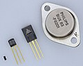
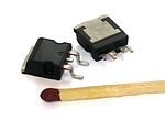
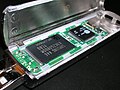
A transistor is a semiconductor device used to amplify or switch electrical signals and power. It is one of the basic building blocks of modern electronics...
100 KB (10,419 words) - 05:39, 6 October 2024
junction transistor (BJT) is a type of transistor that uses both electrons and electron holes as charge carriers. In contrast, a unipolar transistor, such...
55 KB (6,795 words) - 12:20, 17 August 2024
Three-dimensional integrated circuit (redirect from 3D IC)
local (transistor) level. In general, 3D integration is a broad term that includes such technologies as 3D wafer-level packaging (3DWLP); 2.5D and 3D interposer-based...
81 KB (8,773 words) - 07:39, 27 August 2024
MOSFET (redirect from Metal oxide semiconductor field-effect transistor)
metal–oxide–semiconductor field-effect transistor (MOSFET, MOS-FET, MOS FET, or MOS transistor) is a type of field-effect transistor (FET), most commonly fabricated...
99 KB (11,949 words) - 03:16, 29 September 2024
Transistor aging (sometimes called silicon aging) is the process of silicon transistors developing flaws over time as they are used, degrading performance...
3 KB (362 words) - 05:13, 31 July 2024
A transistor is a semiconductor device with at least three terminals for connection to an electric circuit. In the common case, the third terminal controls...
68 KB (7,622 words) - 03:13, 29 September 2024
bipolar transistors with the emitter of one transistor connected to the base of the other, such that the current amplified by the first transistor is amplified...
9 KB (1,317 words) - 18:29, 28 August 2024
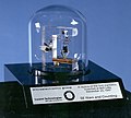
The point-contact transistor was the first type of transistor to be successfully demonstrated. It was developed by research scientists John Bardeen and...
7 KB (904 words) - 16:02, 27 August 2024

Integrated circuit (section ULSI, WSI, SoC and 3D-IC)
are constructed using many different technologies, e.g. 3D IC, 2.5D IC, MCM, thin-film transistors, thick-film technologies, or hybrid integrated circuits...
87 KB (9,261 words) - 08:32, 27 September 2024

Moore's law is the observation that the number of transistors in an integrated circuit (IC) doubles about every two years. Moore's law is an observation...
104 KB (10,692 words) - 15:53, 25 September 2024

An insulated-gate bipolar transistor (IGBT) is a three-terminal power semiconductor device primarily forming an electronic switch. It was developed to...
38 KB (4,400 words) - 18:57, 6 October 2024
A thin-film transistor (TFT) is a special type of field-effect transistor (FET) where the transistor is made by thin film deposition. TFTs are grown on...
29 KB (3,134 words) - 04:12, 21 September 2024

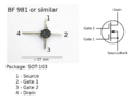
JFET (redirect from Junction Field-Effect Transistor)
The junction field-effect transistor (JFET) is one of the simplest types of field-effect transistor. JFETs are three-terminal semiconductor devices that...
20 KB (2,415 words) - 14:30, 7 June 2024
Flash memory (redirect from 3D NAND)
shrinking the size of the transistors or cells, however the industry can avoid this and achieve higher storage densities per die by using 3D NAND, which stacks...
188 KB (17,256 words) - 06:56, 22 September 2024

CMOS (redirect from CMOS transistor)
/siːmɑːs/, /-ɒs/) is a type of metal–oxide–semiconductor field-effect transistor (MOSFET) fabrication process that uses complementary and symmetrical pairs...
57 KB (6,544 words) - 23:54, 30 September 2024

memory cells. Modern random-access memory (RAM) uses MOS field-effect transistors (MOSFETs) as flip-flops, along with MOS capacitors for certain types...
28 KB (3,022 words) - 03:14, 29 September 2024
A unijunction transistor (UJT) is a three-lead electronic semiconductor device with only one junction. It acts exclusively as an electrically controlled...
9 KB (1,179 words) - 04:49, 2 June 2024
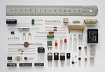
Electronic component (section Transistors)
transistor) Composite transistors BiCMOS (bipolar CMOS) IGBT (Insulated-gate bipolar transistor) Other transistors Bipolar junction transistor (BJT...
26 KB (2,806 words) - 21:23, 27 August 2024
A diffused junction transistor is a transistor formed by diffusing dopants into a semiconductor substrate. The diffusion process was developed later than...
5 KB (589 words) - 03:26, 31 July 2024

Semiconductor device (section Transistor)
by Dawon Kahng and Simon Sze in 1967. FinFET (fin field-effect transistor), a type of 3D multi-gate MOSFET, was proposed by H. R. Farrah (Bendix Corporation)...
37 KB (5,431 words) - 03:17, 29 September 2024

Electronic symbol (section Transistors)
electronic devices or functions, such as wires, batteries, resistors, and transistors, in a schematic diagram of an electrical or electronic circuit. These...
21 KB (1,554 words) - 06:40, 23 September 2024

invented the first gate-all-around (GAA) MOSFET (GAAFET) transistor, an early non-planar 3D transistor, in 1988. Masuoka attended Tohoku University in Sendai...
11 KB (1,003 words) - 03:39, 31 July 2024
2 nm process is the next MOSFET (metal–oxide–semiconductor field-effect transistor) die shrink after the 3 nm process node. The term "2 nanometer", or alternatively...
30 KB (2,512 words) - 03:21, 28 September 2024

random-access memory (DRAM) allowed replacement of a 4 or 6-transistor latch circuit by a single transistor for each memory bit, greatly increasing memory density...
58 KB (5,935 words) - 04:36, 3 October 2024
Amplifier (redirect from Transistor amplifier)
until the transistor provided smaller and higher quality amplifiers in the 1950s. The first working transistor was a point-contact transistor invented...
56 KB (7,058 words) - 18:53, 20 June 2024

An organic field-effect transistor (OFET) is a field-effect transistor using an organic semiconductor in its channel. OFETs can be prepared either by vacuum...
27 KB (3,363 words) - 03:17, 29 September 2024